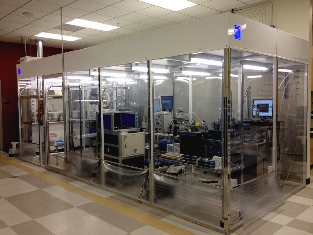
Wafer Bonding Laboratory
Wafer bonding technology offers significant advantages for synthesis of hetero-junctions that cannot be usefully synthesized by more familiar methods such as epitaxial growth techniques. Materials with large misfits or different lattice structures across interfaces can be bonded without causing defect formation in the crystals adjacent to the bonded interfaces. Our interface synthesis instrumentation design utilizes surface research techniques to measure and control substrate and interface chemistry within limits necessary to make hetero-junction devices.
- Custom-designed UHV wafer bonding cluster tool
- Bonds up to 20 kN at temperatures up to 1,200 ˚C
- Ultra high vacuum (down to 10-10 mbar)
- Analysis: AES, RHEED
- e-beam deposition: 2 sources
- Sputter deposition: 2 sources
- Road-lock

- EVG 501
- Up to 150 mm wafers
- Bonds up to 5 kN force at temperatures up to 450 ˚C
- High vacuum (down to 10-5 mbar)
- EVG 520
- Up to 200 mm wafers
- Bonds up to 7 kN force at temperatures up to 550 ˚C
- High vacuum (down to 10-5 mbar)
- Plasma Activation Tool: ACT-300M
- For wafer surface activation
- Multiple wafers in a single process cycle

