
GaN on Si by Wafer Bonding for High Power Devices
GaN is a key material for high power and optoelectronic devices due to its excellent intrinsic properties such as wide bandgap and high electron mobility. GaN-based devices are mostly fabricated by growing GaN thin films on suitable substrates such as SiC and Sapphire. Due to the cost and the small size of those SiC and Sapphire substrates, research efforts on growing GaN thin fims on less-expensive and large area Si substrates are increasing. However, the quality of those GaN thin films grown on Si is still hampered by high defect density due to mismatch in lattice structure, lattice constant and thermal mismatch.
In this project, we fabricate the GaN(0001) on Si(100) by wafer bonding and layer transfer techniques and electrical devices, such as Si-MOSFET and GaN-HEMT, on the integrated GaN on Si(100). We also characterize the nanostructure, chemical and electrical properties of the integrated structures to be optimized for high power device applications.
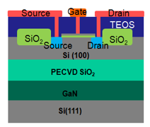
Cross-Section of n-MOSFET on the transferred
Si(100) on GaN/Si(111).
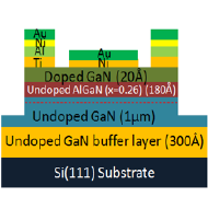
Layer structure for GaN HEMT fabrication on a Silicon substrate.
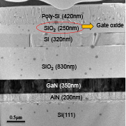
Cross-sectional TEM image of the integrated
Si(100)/SiO2/GaN/Si(111).