
Atomic Scale Characterization of TI, TMD and Graphene-based Devices, SWAN 2.0
The objective of this task is to correlate the physical properties of the materials, including integrated multi-layers and devices fabricated by particular processes, with their nanostructure and chemical properties. We use various high resolution TEM-based techniques to characterize the growth morphology of 2D materials of interest.
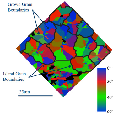
Crystallographic orientation map of a CVD grown graphene, showing its grain morphology.
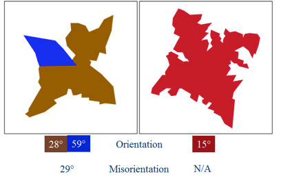
Orientation of individual grown graphene grains.