
Aberration-corrected Microscopy of 2D Materials and Devices, LEAST
The objective of this task is to provide the fundamental understanding of chemical vapor deposition (CVD) growth and synthesis of large area 2D materials using high-resolution, aberration corrected transmission electron microscopy. Interfacial defects such as misfit dislocations and surface steps or ledges, growth defects, interface morphology (e.g., sharp or diffuse interface), interfacial reaction products, and interfacial strains are also characterized.
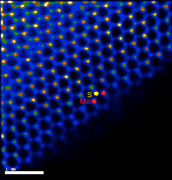
Atomic resolution STEM HAADF image of the transferred MoS2, identifying the location of Mo and S atoms and their 2H stacking sequence.
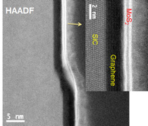
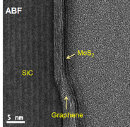
Cross-sectional HAADF (left) and ABF (right) STEM images of MoS2 layers grown on graphene/SiC. HAADF image highlights the MoS2 layer and its coverage over the surface step, whereas ABF image enhances the contrast of the graphene layers.